


Tampilan:1 创始人: Site Editor Publish Time: 2026-08-30 Origin: Site


Abstract
As the core soldering process for batch
assembly of through-hole printed circuit boards, wave soldering is widely used
in the electronics manufacturing production process due to its high production
efficiency and suitability for mass manufacturing. Solder bonding (bridging) is
a soldering defect that occurs frequently during wave soldering production.
This defect occurs when two or more electrically isolated solder joints are
connected by solder, directly causing electrical short-circuit faults on circuit
boards and seriously affecting the yield and reliability of electronic
products. This paper analyzes the mechanism of solder bonding defects from
multiple dimensions including soldering temperature, preheating process, flux,
equipment parameters, PCB design, component assembly, and solder quality, and
proposes corresponding process optimization and improvement plans, providing
reference ideas for solving the problem of poor solder soldering in the
electronics manufacturing industry.
Keywords:
wave soldering; soldering; bridging; printed circuit board; soldering defects;
process optimization
1. Introduction
Modern electronic equipment is continuously
developing towards miniaturization and integration, with increasing component
layout density on printed circuit boards (PCBs), which places higher demands on
the stability of wave soldering processes. Wave soldering relies on molten
solder to form flowing peaks that contact the bottom solder joints of the PCB
to complete the soldering operation. In mass continuous production mode, due to
the coupling of multiple factors such as equipment status, process parameters,
material characteristics, and PCB design, various soldering defects such as
solder joints, cold solder joints, missed soldering, and solder balls are
highly likely to occur. Among these, solder defects directly cause circuit
short circuits. If they flow into downstream finished product processes, they
not only cause product failure but also increase repair costs and restrict
production efficiency. Therefore, systematically identifying the triggering
factors for wave soldering defects and implementing targeted improvement
measures is of practical engineering significance for enhancing PCB assembly
soldering quality.
2. Analysis of the main causes of wave
soldering defects
The essence of tin is the phenomenon where
molten solder unexpectedly spreads and migrates between solder joints, forming
conductive bridging after cooling. The defects are often not caused by a single
factor but are the result of the combined effects of process, material, and
structural design.
2.1 Improper control of solder melting
temperature
Solder temperature is a key process parameter affecting the surface tension and flowability of solder. When the solder bath temperature is set too high, the surface tension of the molten solder decreases, significantly enhancing flowability. At the moment the wave peaks contact the PCB, low-tension liquid solder is more likely to spread between adjacent pads and component pins, preventing timely shrinkage separation before cooling, and after cooling and curing, solder bridging forms between solder joints. However, solder temperature cannot be simply lowered; too low temperatures can lead to cold solder joints and other soldering defects, and temperature range imbalance is a common adverse factor on site.
2.2 Insufficient PCB preheating process
The preheating process in wave soldering
activates the flux and reduces the temperature difference under PCB heating. If
the preheating temperature is too low or the preheating time is insufficient,
the body temperature of the PCB substrate, pads, and component pins is much
lower than the molten solder temperature. When the PCB contacts wave solder,
the temperature difference between hot and cold is too large, causing abnormal
fluidity changes after the solder contacts the low-temperature workpiece; At the
same time, the flux cannot be fully activated, causing uncontrolled solder
wetting, with liquid solder easily overflowing to surrounding areas, increasing
the probability of solder bonding between adjacent pins and pads. Conversely,
excessive preheating can also cause flux to evaporate and fail prematurely,
also triggering poor soldering, so the preheating window must be precisely
controlled.
2.3 Flux quality and spraying amount
abnormalities
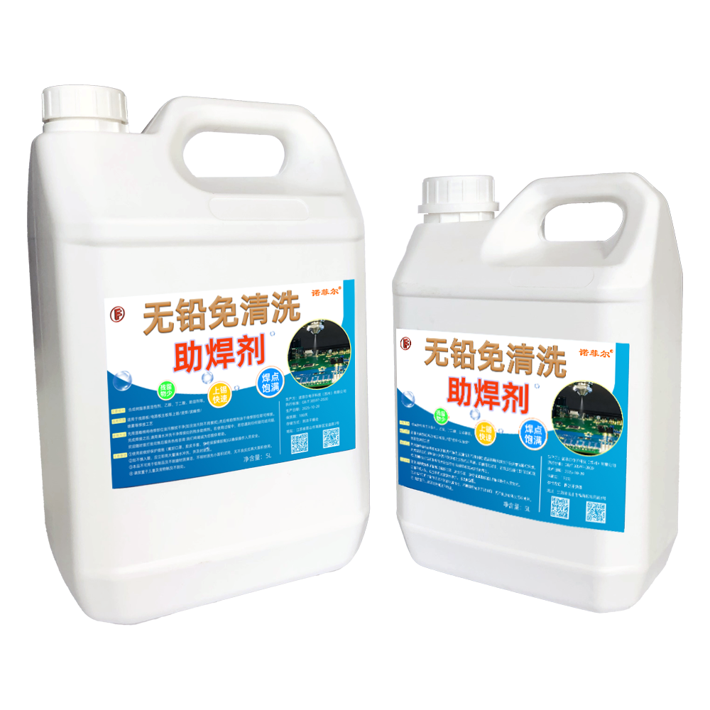
The main function of flux is to remove the
oxide layer on the surfaces of pads and pins, improving solder wetting
performance. On one hand, excessive flux spraying causes excess liquid flux to
accumulate in the gaps between pads at the bottom of the PCB, causing molten
solder to diffuse along the flux spread path to adjacent solder joints; On the
other hand, if the flux itself does not meet physical and chemical quality
standards and the active component ratio is unbalanced, it excessively
increases solder wetting fluidity and promotes solder spread across solder
joints. Additionally, uneven flux spraying and localized accumulation can also
cause concentrated solder interconnection issues in certain areas.
2.4 Unreasonable process parameters for
peak height
Wave height determines the contact depth
and contact area between the PCB and molten solder. If the peak height is set
too high, the PCB immersed too deeply in the solder peaks increases the contact
range between the solder and the PCB bottom solder joints and pins, making it
easier for liquid solder to fill the gaps between the pins; At the moment the
PCB peels off the wave, the solder cannot rely on its own surface tension to
complete separation and breaking, leaving residual solder to connect adjacent
solder joints, resulting in batch solder connection defects. Too low a wave
height can cause missed solder joints and poor pad wetting, requiring parameter
tuning to match the board thickness and component type.
2.5 PCB pad structural design defects
PCB hardware design is the fundamental
influencing factor. When the spacing between pin pads is too small and the
physical gap between solder joints is insufficient, leaving limited space for
solder retraction and separation, bridging is very likely to occur under
conditions with high solder flow; Unreasonable pad size design, such as pads
being too large, can also expand the solder spread range. If high-density
through-hole boards are not adequately designed during the initial design phase
and do not fully consider wave soldering process compatibility, it is difficult
to completely eliminate the risk of solder bonding by simply adjusting
equipment parameters later.
2.6 Component Assembly Positioning
Deviation
The assembly accuracy of component inserts
directly affects the position of the pins relative to the pads. During
insertion operations, if the component pins shift toward the center of the pad,
the pins are skewed or offset on one side, and the pins encroach on the gap
space between adjacent pads. During soldering, molten solder spreads outward
along the offset pins, crossing to adjacent solder joints, and after cooling
and curing, forms a continuous solder connection. This issue occurs frequently
in production scenarios where the precision of the insertion equipment is
insufficient and manual insertion operations are used.
2.7 Accumulation of impurities inside
the solder tank
After long-term continuous production and
use, various impurities such as copper and metal oxides may mix into the solder
tank. These impurities alter the physical properties of the molten solder,
destroying its original surface tension and wettability, and causing
deterioration of solder fluidity and cohesion. At this time, the fracture
effect of solder decouples from the waves, making it easy to cause wire drawing
and solder drag, which can lead to solder bonding between adjacent solder
joints—a hidden factor that is often overlooked in long-term production.
3. Countermeasures for Improving Wave
Soldering Defects
For the above various triggering factors,
the approach of "prioritizing source design, assisted by process parameter
optimization, and ensuring regular equipment maintenance" should be
followed, and improvement plans should be implemented in combination with
actual on-site production conditions.
3.1 Reasonably control the working
temperature range of the solder
Strictly set the solder bath temperature
according to solder alloy specifications, combined with PCB thickness and
component heat resistance ratings, to keep the solder temperature within the
specified process range and avoid ultra-high temperature operation. During
production, regularly monitor the actual temperature of the solder bath to
avoid deviations between the displayed temperature and the actual molten solder
temperature; Temperature adjustment uses a small, stepwise adjustment method,
synchronizing soldering status to ensure wetting effects and prevent secondary
defects such as cold solder joints and cold solder joints introduced to solve
solder bonding.
3.2 Optimize the process conditions of
the preheating system
Adjust the temperature and conveying speed
of the wave soldering preheating section to ensure that before the PCB enters
the solder peak, the board surface, pads, and pins can be evenly heated,
ensuring flux is fully activated and minimizing the temperature difference
between the workpiece and molten solder. For circuit boards with large heat
retention such as thick and multilayer boards, appropriately match preheating
power to reduce temperature differences across different areas of the board; At
the same time, avoid excessive preheating to prevent flux from evaporating
prematurely and losing soldering function. A temperature curve tester can be
used to collect the actual PCB heating curve and quantify and control the
preheating process.
3.3 Control flux quality and spray
amount
Select qualified flux products that meet
process standards and have stable performance, and prioritize matching models
specifically for wave soldering processes. Conduct regular inspections of the
flux spraying system, adjust spraying pressure and nozzle position to ensure
uniform flux spraying, strictly control spray thickness, and eliminate local
flux buildup; Clean the printheads regularly to prevent blockages and uneven
spraying. If solder is concentrated and outbreaks, try slightly reducing flux
supply and compare and observe changes in soldering quality.
3.4 Scientifically adjust the peak
working height
Adjust the wave peak height according to
PCB thickness and component lead length, controlling the reasonable depth of
PCB immersion in the wave peak, and reducing unnecessary solder contact area.
At the same time, pay attention to the operating status of the wave motor to
ensure the wave liquid level is stable and free from severe turbulence;
excessive turbulence can also worsen solder spread. Considering soldering
penetration, while ensuring the solder joints are fully wet, try to minimize
the risk of solder connection caused by excessive wave peaks.
3.5 Optimize PCB pad process design
Conduct Manufacturability Analysis (DFM)
during the PCB design phase to fully adapt to wave soldering requirements. Set
reasonable safety spacing between through-hole pads to avoid spacing too small;
Optimize pad hole diameter and dimensions, and, if necessary, use pad openings
designed to prevent solder connection to reduce the probability of bridge
defects at the hardware source. For high-density circuit boards, if conditions
permit, local use of masking tooling and other auxiliary process methods can
also be considered.
3.6 Improving Component Insert
Positioning Accuracy
Automated insertion equipment is regularly
calibrated to maintain the accuracy of movement mechanisms, reducing issues of
component pin misalignment and skewing; Manual insertion stations should
improve operational standards, strengthen employee training, and ensure
component pins are centered and placed in the pad holes. During production,
inspection frequency has been increased to promptly intercept semi-finished
products with severe pin misalignment from entering the soldering process,
reducing poor solder bonding caused by assembly issues.
3.7 Implement daily maintenance of
solder tanks and solder quality control
Establish a solder tank maintenance system,
regularly remove oxidized slag from the surface of the solder tank, and conduct
sampling and testing of the solder composition according to cycles. When
impurity content inside the solder exceeds the standard, promptly replace the
solder or perform impurity removal to ensure stable melt soldering performance.
This reduces damage to the surface tension of the solder by impurities,
improves the fracture characteristics of the solder when it leaves the peak,
and decreases solder defects caused by solder drag and wire drawing.
4. Conclusion
Wave soldering defects are process issues
caused by multi-factor coupling, and defects in on-site production are rarely
caused by a single cause. When batch solder defects occur, it is not enough to
adjust just one equipment parameter; temperature curve records, PCB design
documents, material inspection results, and equipment operation records should
be comprehensively investigated. Priority should be given to easily adjustable
items such as equipment process parameters and material quality. For repeatedly
unresolved defects, trace back PCB design and upstream insertion processes.
Through multidimensional coordinated control of design, process, and equipment
maintenance, the occurrence of tinning defects can be effectively suppressed,
improving wave soldering yield, reducing the cost of electronic product
repairs, and ensuring the quality of circuit board assembly.
 Su Gongwang Security 32058302004438